Nanofabrication deals with the fabrication of materials and structures at nanoscale. The essential requirements of a nanofabrication are a clean room which is devoid of particles and contaminations and also a specially designed equipment facility for thin film deposition, patterning and etching. We are all familiar with integrated chips (ICs). ICs are manufactured through nanofabrication by placing transistors and interconnections between the transistors. Similarly, the magnetoresistive random access memory (MRAM) comprised of transistors and interconnections to its fundamental unit called magnetic tunnel junction (MTJ). As MRAM make use of magnetic states of its fundamental unit called magnetic tunnel junction (MTJ) to store information, it is devoid of power loss and hence offers excellent scalability and affable integration to chip fabrication processes.
How to manufacture/fabricate an MRAM?
The IC manufacturing process can be understood through two subcategories, the stage where the transistors are implemented called front-end-of-the line (FOEL) and a space where the interconnects are created within a device is termed as back-end-of-the-line (BOEL). Interconnects are the tiny wiring scheme employed in device fabrication. The BOEL often employs two types of interconnects, the intermediate wires for the lower-level connection and the global wires which connect the intermediate layers. The simplicity of MRAM lies on the fact that it allows the designers to embed them in BEOL logic circuitry.
MRAM fabrication usually follows the BOEL processes in semiconductor fabrication. The process steps in BOEL are categorized into two main categories, the patterning and the dual damascene process. In the process flow, patterning is used to establish the required wiring scheme. The dual damascene process typically contains three major parts. The first step is called metallization in which a diffusion barrier is created by etching followed by a via dielectric deposition. The low k-dielectrics which is a dielectric material with smaller dielectric constant as compared to that of silicon dioxide and capping layer are the other two important parts in the dual damascene process. The seed and capping layer is formed by tantalum and tantalum nitrides respectively using a physical vapor deposition technique.
Let’s understand the key procedures of MRAM fabrication step by step.
1. Formation of bottom electrode (BE)
The bottom electrode has to form by following patterning as the key step. Patterning is done in such a way to accommodate the layer deposition at the vias and trenches simultaneously. This particular patterning method is called dual damascene process as explained. The bottom electrode of MRAM has to be defect free and it has to be formed in a way to provide ultra-smooth surface for the deposition of MTJ stack layer with predesigned planarization. Hence, maintaining the smoothness of BE as well as final height of the electrode to specific level is crucial to ensure quality device performance.
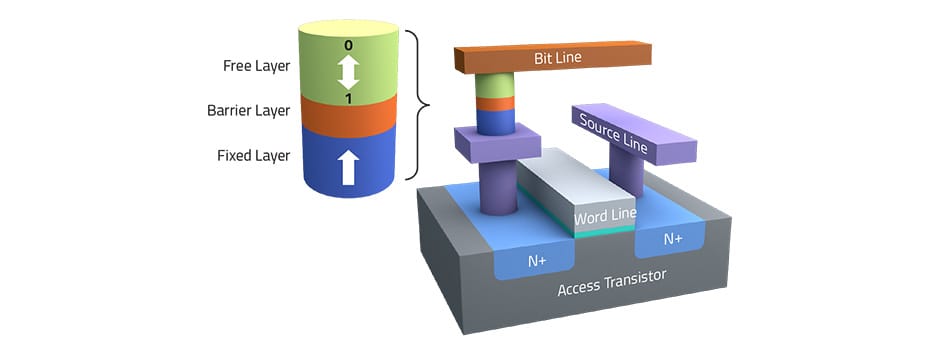
2. Stack formation of MTJ
MRAM stack deposition stage employs an integrated physical vapor deposition cluster tool for the deposition of different metal and insulator layers, typically in the range of thickness 0.5-5 nm. A widely used material to form the insulating layer between the free layer and fixed (reference) layer is magnesium oxide (MgO) thin film. Each layer has to be optimized in terms of stoichiometry, roughness, uniformity and thickness. The tunnel magnetoresistance (TMR) and resistance-area product (RA) are the parameters crucial to ensure the device performance. The precision of deposition has to be monitored frequently in order to maintain the TMR characteristics and also to obtain the pre designed RA.
3. Magnetic annealing
In the magnetic annealing stage of stack deposition, the MTJ is annealed at a higher temperature in the presence of an external magnetic field. In this stage, focus has to be provided to ensure the quality of interface and individual thin film layers. The magnetic orientation and electrical properties of MTJ has to be monitored after the annealing process for process control.
4. Patterning for MTJ
In patterning stage, patterns are created within the circularly shaped pillars of MRAM in order to obtain a required MTJ structure. MRAM fabrication uses lithography to make useful patterns of required MTJ stack. The patterning process involves transfer of patterns from mask to a material which is sensitive to electron beam or light, called photoresist and transfer from photoresist to MTJ stack. Material redeposition along the exposed portion of insulating layer and etch corrosion are the key factors need to me monitored and minimized during this stage. The switching distribution of MRAM cells are impacted by the uniformity of cell patterning. A defect free encapsulation layer with specific thickness covers the device and provide necessary protection for the MTJ structure.
5. Formation of top electrode (TE)
The bottom electrode has to form by following patterning as the key step. Patterning is done in such a way to accommodate the layer deposition at the vias and trenches simultaneously. This particular patterning method is called dual damascene process as explained. The bottom electrode of MRAM has to be defect free and it has to be formed in a way to provide ultra-smooth surface for the deposition of MTJ stack layer with predesigned planarization. Hence, maintaining the smoothness of BE as well as final height of the electrode to specific level is crucial to ensure quality device performance.
Despite the challenges associated with fabrication steps, identifying materials for MRAM with good thermal stability, lower damping constant, higher anisotropy, larger spin hall effect and demonstrated Rashba effect are with utmost consideration. Building machine learning models to optimize the design parameters for MRAM fabrication can also be an effective approach to overcome the device failure mechanisms associated with fabrication.