Transmission Electron Microscopy (TEM) is a powerful technique used to visualize the internal structure of materials at the nanometer scale. Unlike conventional light microscopy, which uses visible light to illuminate samples, TEM employs a beam of electrons, allowing for much higher resolution imaging
Electrons to Generate High resolution Image
TEM employs a beam of electrons, enabling much higher resolution imaging due to the shorter wavelength of electrons compared to visible light. Electrons have significantly smaller wavelengths than photons, allowing them to resolve much finer details in the sample structure. This results in improved spatial resolution, enabling the visualization of atomic-scale features in materials.Additionally, electrons interact more strongly with matter than photons, providing valuable information about the sample’s composition and properties. Overall, the use of electron beams in TEM offers unparalleled capabilities for studying the nanoscale world with exceptional detail and precision.
Principle of Operation
In Transmission Electron Microscopy (TEM), a beam of electrons is transmitted through an ultra-thin sample. These electrons interact with the atoms within the sample, providing valuable information about its structure, composition, and properties.
Electron Interaction
As the electron beam passes through the sample, it undergoes various interactions, including scattering, diffraction, and absorption. These interactions occur due to the interaction between the electrons and the atoms in the sample.
Scattering
Electron scattering refers to the deviation of the electron trajectory as it interacts with the atoms in the sample. This scattering can be elastic, where the electrons retain their energy, or inelastic, where energy is transferred to the sample.
Diffraction
Electron diffraction occurs when the electrons are diffracted by the crystalline lattice of the sample. This phenomenon produces diffraction patterns that can reveal information about the crystal structure of the material, including lattice spacing and orientation.
Absorption
Some electrons in the beam may be absorbed by the sample as they pass through. The extent of absorption depends on the thickness and composition of the sample, as well as the energy of the electrons.
Imaging
The interactions between the electrons and the sample are captured by detectors, producing high-resolution images of the internal structure of the material. These images provide detailed information about the arrangement of atoms, defects, grain boundaries, and other features.
Analysis
In addition to imaging, TEM allows for various analytical techniques, such as electron diffraction and energy-dispersive X-ray spectroscopy (EDS). Electron diffraction patterns can be used to determine the crystal structure of the material, while EDS provides elemental analysis of the sample
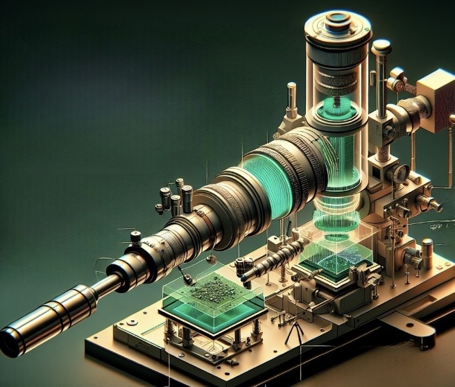
Components of Transmission Electron Microscope (TEM)
Transmission Electron Microscopes (TEMs) consist of several essential components that work together to generate high-resolution images of samples at the atomic scale.
Electron Source
The electron source emits a beam of electrons, which serves as the primary imaging tool. This beam can be generated through thermionic emission or field emission processes.
In thermionic emission, electrons are emitted from a heated filament, while in field emission, electrons are emitted from a sharp tip subjected to a strong electric field.
The electron source provides a steady supply of electrons for imaging, with the beam intensity and stability being crucial for achieving high-quality images.
The choice of electron source depends on factors such as the desired beam intensity, stability, and resolution.
Overall, the electron source is a critical component of TEM, providing the primary imaging beam necessary for visualizing samples at the atomic scale.
Electron Lenses
Electron lenses focus and manipulate the electron beam to achieve high-resolution imaging. They consist of magnetic coils that produce magnetic fields to bend and focus the electrons.These lenses include condenser lenses, which focus the beam onto the sample, and objective lenses, which form an image of the sample.
Condenser lenses ensure that the electron beam is properly focused onto the sample, optimizing image resolution and clarity.Objective lenses play a crucial role in forming an image of the sample by magnifying the electron beam and projecting it onto a detector.
By manipulating the electron beam, electron lenses enable TEM to achieve high-resolution imaging of samples at the atomic scale.
Sample Holder
The sample holder is where the sample is mounted for analysis. It must be compatible with high vacuum conditions and allow precise positioning of the sample relative to the electron beam. Sample holders often include mechanisms for tilting and rotating the sample for different imaging angles.
Vacuum System
The vacuum system in TEM is essential for creating a high vacuum environment within the microscope chamber. This vacuum prevents electron scattering and absorption by air molecules, ensuring the transmission of electrons through the sample for imaging.
The vacuum system consists of pumps and valves that remove air and other gases from the microscope chamber. These pumps create and maintain the necessary vacuum level, typically in the range of $10^{-6}$ to $10^{-9}$ torr, conducive to electron transmission.
By eliminating air molecules, the vacuum system minimizes electron interactions that could degrade image quality or distort sample features. This enables the TEM to achieve high-resolution imaging of samples at the atomic scale.
Overall, the vacuum system is a critical component of transmission electron microscopy, providing the low-pressure environment necessary for optimal imaging performance
Detectors
Detectors in TEM capture signals generated by interactions between the electron beam and the sample. These signals include transmitted electrons for imaging and diffracted electrons for diffraction analysis.
Various types of detectors can be used in TEM, including photographic film, phosphor screens, and digital cameras. Each type of detector has its advantages and limitations in terms of sensitivity, resolution, and dynamic range.
Transmitted electron detectors capture electrons that pass through the sample without being scattered or absorbed. They form high-resolution images of the sample’s internal structure, providing details at the atomic scale.
Diffracted electron detectors capture electrons that have undergone diffraction by the sample. These detectors produce diffraction patterns that provide information about the crystal structure, orientation, and defects within the sample.
Detectors in TEM play a crucial role in capturing and recording the signals necessary for image formation and analysis. They enable researchers to visualize and study the structural and chemical properties of materials with exceptional detail and p
Control and Imaging System
The control and imaging system consists of electronics and software that control microscope functions and acquire images. Users can adjust imaging parameters such as magnification, focus, and brightness, as well as perform image processing and analysis.
During the imaging process, the electron source emits a beam, which the electron lenses focus onto the sample. The sample then interacts with the electron beam, and detectors capture the resulting signals. Through the control and imaging system, users can adjust parameters and acquire high-resolution images of the sample.
Each component of the transmission electron microscope plays a vital role in facilitating the imaging process, from generating and manipulating the electron beam to capturing and analyzing signals from the sample.
Principle of X-ray Spectroscopy
X-ray spectroscopy is a technique used to analyze the chemical composition and electronic structure of materials by measuring the energy and intensity of X-rays emitted or absorbed by the sample. The principle behind X-ray spectroscopy is based on the interaction between X-rays and the inner-shell electrons of atoms within the sample.
When an X-ray beam interacts with the sample, it can cause inner-shell electrons to be ejected from their orbits, creating vacancies in the electron shells. These vacancies are filled by electrons from higher energy levels, resulting in the emission of characteristic X-rays with energies corresponding to the energy difference between the initial and final electron states.
By analyzing the energies and intensities of these characteristic X-rays, scientists can identify the elements present in the sample and determine their concentrations. Additionally, X-ray spectroscopy can provide information about the chemical bonding environment, oxidation states, and electronic structure of the atoms within the sample.
Relationship of X-Ray Spectroscopy with TEM
Transmission Electron Microscopy (TEM) and X-ray spectroscopy are complementary techniques that are often used together for comprehensive materials characterization.
In TEM, electron beams are transmitted through thin samples, allowing for high-resolution imaging of the sample’s internal structure. TEM provides detailed information about the morphology, crystal structure, and defects within the sample at the atomic scale.
X-ray spectroscopy, on the other hand, provides chemical and elemental analysis of the sample’s composition. By analyzing the characteristic X-rays emitted or absorbed by the sample, scientists can identify the elements present and their chemical environments.
The combination of TEM and X-ray spectroscopy allows researchers to correlate the structural and chemical information obtained from both techniques, providing a more comprehensive understanding of the material under investigation. For example, TEM can identify specific features within a sample, such as nanoparticles or grain boundaries, while X-ray spectroscopy can determine the elemental composition and chemical states of these features.
Overall, the integration of X-ray spectroscopy with TEM enhances the capabilities of both techniques and enables researchers to obtain valuable insights into the structure-property relationships of materials.
Applications of Transmission Electron Microscopy
TEM finds applications across various fields, owing to its ability to visualize samples at the atomic scale and provide detailed information about their structure and composition.
Materials Science: In materials science, TEM is used to study the microstructure of materials, including metals, ceramics, polymers, and composites. It helps researchers understand defects, grain boundaries, phase transformations, and other critical features that influence material properties.
Nanotechnology: TEM plays a vital role in nanotechnology by enabling the characterization of nanomaterials such as nanoparticles, nanowires, and carbon nanotubes. It allows researchers to investigate size, shape, and distribution of nanoparticles, essential for designing nanomaterials with tailored properties.
Biology and Biomedical Research: In biology and biomedical research, TEM is used to study the ultrastructure of biological samples, including cells, tissues, and biomolecules. It provides insights into cellular organelles, protein structures, virus morphology, and other biological phenomena at the nanoscale.
Semiconductor Physics: TEM is indispensable in semiconductor physics for analyzing the structure and defects in semiconductor materials and devices. It helps characterize thin films, interfaces, dopant distributions, and device structures, essential for semiconductor device fabrication and optimization.
Catalysis: In catalysis research, TEM is used to investigate the structure and morphology of catalyst nanoparticles, providing insights into their catalytic activity and selectivity. It helps researchers design more efficient catalysts for various chemical reactions, including those used in energy production and environmental remediation.
Environmental Science: TEM is employed in environmental science to study the structure and behavior of nanoparticles in environmental systems. It helps understand processes such as nanoparticle aggregation, transformation, and interaction with contaminants, contributing to the assessment and remediation of environmental pollution.
Advantages and Disadvantages of Transmission Electron Microscopy
Advantages:
- High Resolution: Transmission Electron Microscopy (TEM) offers exceptionally high resolution, allowing imaging of samples at the atomic scale.
- Detailed Structural Information: TEM provides detailed information about the internal structure of materials, including crystal structure, defects, and interfaces.
- Elemental Analysis: TEM can be coupled with energy-dispersive X-ray spectroscopy (EDS) for elemental analysis, enabling identification of elements present in the sample.
- Versatility: TEM can analyze a wide range of materials, including metals, ceramics, polymers, biological samples, and nanomaterials.
- Real-time Imaging: Advanced TEM techniques such as in-situ TEM enable real-time imaging of dynamic processes, such as phase transformations and chemical reactions.
Disadvantages:
- Sample Preparation: Sample preparation for TEM can be time-consuming and technically challenging, requiring thinning of samples to less than 100 nanometers in thickness.
- High Vacuum Requirement: TEM operates under high vacuum conditions, limiting the types of samples that can be analyzed and potentially causing sample degradation.
- Complexity and Cost: TEM is a complex and expensive instrument, requiring specialized training and maintenance, as well as significant initial investment.
- Electron Beam Damage: High-energy electron beams used in TEM can cause radiation damage to samples, altering their structure and composition.
- Limited Depth of Field: TEM has a limited depth of field, which can make imaging thick samples or three-dimensional structures challenging.
Conclusion
TEM stands as a powerful tool for investigating the structure and properties of materials at the atomic scale. Its high resolution, coupled with its ability to provide detailed structural and chemical information, makes it indispensable across various fields, from materials science to biology and nanotechnology.
Despite challenges such as sample preparation and equipment complexity, the wealth of information TEM provides has propelled scientific advancements and technological innovations.
As research continues to push the boundaries of what is possible, TEM remains at the forefront, driving our understanding of the nanoworld and shaping the future of science and technology.